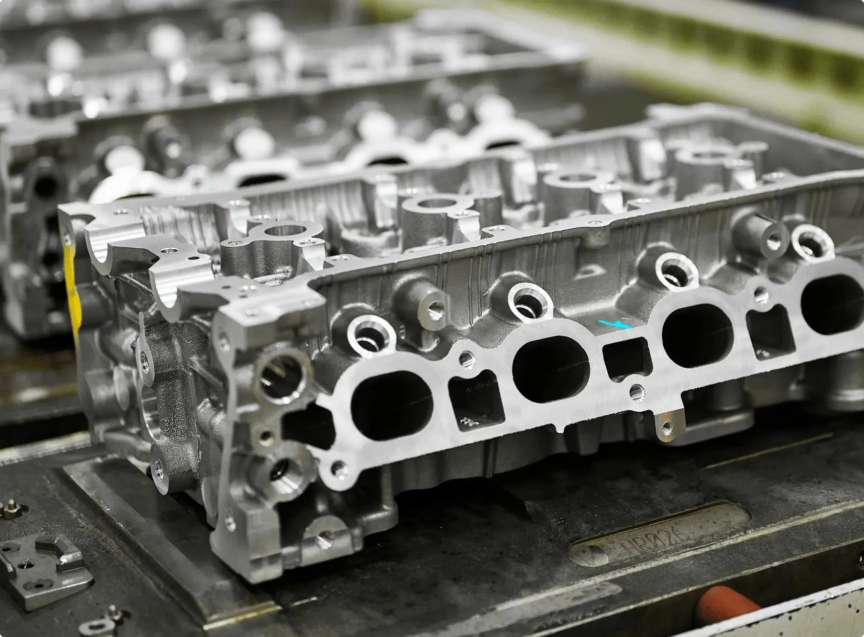
Photolithography is the central process in semiconductor fabrication, used to transfer circuit patterns onto silicon wafers with extreme accuracy and repeatability. It enables the production of tiny features and high transistor densities essential for modern devices, making lithography a core driver of both performance and yield in semiconductor manufacturing.
As physical scales shrink and feature densities increase, the mechanical design of photolithography equipment (like how components are fastened and maintained) becomes increasingly important. Material properties, surface coatings and joint geometry all intersect to influence machine stability, cleanliness and overall reliability.
The mechanical demands of photolithography equipment
The systems involved with photolithography tools (precision optics, motion stages, environmental control systems) need to operate together seamlessly without error. The wafer stage, for example, must move and position substrates with sub-micron precision, meaning even tiny mechanical instability can affect pattern placement and yield.
In this context, the mechanical support infrastructure which includes joints and threaded interfaces must:
-
Maintain ultra-stable assemblies to support high-accuracy stage motion
-
Enable lightweight, vibration-resistant structural designs
-
Preserve cleanliness and precision in tightly controlled environments
-
Support repeatable service and maintenance without degrading performance
Mechanical choices at this level therefore affect both dynamic precision and long-term reliability.
How materials, coatings and geometry affect joint performance
Photolithography machines usually use lightweight alloys and precision-machined components to enable faster motion and tighter control. These materials as well as advanced surface coatings, are chosen for thermal behaviour and weight reduction as much as strength.
However, softer materials are more prone to thread wear and deformation under repeated assembly, especially where engagement length is limited. Alongside this, thin coatings can be damaged by installation processes, reducing corrosion protection or surface performance. Instruments designed for nanometre-scale pattern placement depend on every element of the mechanical stack performing consistently to preserve positional repeatability across millions of cycles.
Why conventional threaded joints create complexity
In many precision assemblies, threads are typically cut directly into the parent material. In photolithography equipment this can lead to multiple issues:
-
Wear during repeated maintenance, degrading mechanical stability over time
-
Inconsistent preload, affecting the stiffness and alignment of critical structures
-
Risk of over-torque, which can deform lightweight alloys or damage coatings
-
Sensitivity to vibration and thermal cycling, which are inherent in high-throughput fabs
Because photolithography processes demand tight tolerances and high uptime, these joint weaknesses can cascade into performance drift or unplanned maintenance.
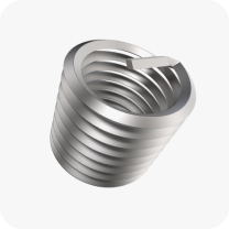
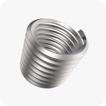
Where Tangless® inserts simplify photolithography assemblies
Tangless® wire thread inserts address these mechanical challenges by providing a dedicated threaded interface that is stronger, more wear-resistant and less sensitive to material variability than conventional threads in parent materials. By separating the functional thread from the substrate itself, Tangless® inserts help mechanical systems meet the demanding precision required in photolithography without sacrificing maintainability. Specifically, they offer:
-
Stable, repeatable threads with consistent preload, supporting precision assemblies
-
Improved wear resistance in lightweight or coated materials, prolonging service life
-
Reduced sensitivity to thermal cycling and vibration, enhancing long-term reliability
-
Cleaner installation and removal, with no tang break-off debris that could compromise cleanliness
-
Simplified maintenance, reducing the risk of joint degradation during servicing
Supporting precision, uptime and long-term reliability
Photolithography tools are capital-intensive and must operate with minimal downtime. Even small mechanical deviations can affect overlay accuracy (the alignment between patterns from successive exposures) reducing yield and increasing costs. Alignment challenges are a central concern in semiconductors as features shrink and tolerances tighten.
Mechanical stability in motion systems, material behaviour under thermal stress, and the ability to clean and rework assemblies without introducing variability are all factors that contribute to up-time and predictable performance in daily operation.
KATO Advanex brings decades of experience delivering wire thread insert technology into the world’s most demanding manufacturing environments. Our Tangless® inserts are designed to support stable, repeatable joints in lightweight, compact and service-critical assemblies. Our solutions can help photolithography equipment maintain performance, reduce maintenance risk and protect long-term uptime. For semiconductor manufacturers seeking reliability at small scales, KATO provides proven solutions built for precision-driven production.


.jpg?width=352&name=EV%20charging%20(3).jpg)